2.5d 3d chip integration
Ad Leaders In Large-Item High Volume 3D Additive Manufacturing Printing Production. Through-silicon via TSV interconnects High density 3D IC applications filled 2-10 µm diameter up to 81 aspect ratio and 10-50 µm pitch Lower density 25D3D package architectures 10-50.

Now You Can Automate Latch Up Verification For 2 5 3d Technologies
There are already quite some applications that use such hybrid assembly techniques.
. Due to yield cost time to market power dissipation and performance considerations 25D and 3D heterogeneous integration of chiplets represent a new phase for Moores Law. ChipletChip is the unit in. As the design complexity grows dramatically in modern circuit designs 25D3D chippackageboard integration has become effective for optimizing system performance and power consumption.
With the advance of 25D and 3D integration there are new ESD challenges but also opportunities for cost reduction. Previous Chapter Next Chapter. Our 25D3D integration technology platform is based on several enabling process modules which include.
Rapid PSI Is The Fastest Additive Manufacturing Source For Prototyping Production Parts. Director Corporate Marketing UMC. Various 25D3D technologies have been explored.
25D3D Supply Chain Integration Between Foundry and OSAT Kurt Huang PhD. 1Q13 MEOL 25D3D chip stacking. Among the explored technologies the wafer-level integrated fan-out InFO package-on-package PoP has been adopted by major companies.
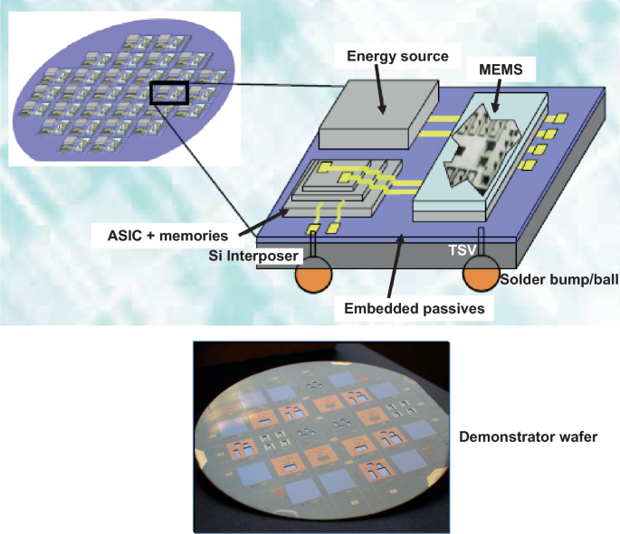
As the design complexity grows dramatically in modern circuit designs 25D3D chippackageboard integration has become a key to beat process limitation for optimizing system performance and power consumption. Chip makers have for instance combined a logic controller chip together with a Microelectromechanical systems MEMS in one. Among many technologies wafer-level chip-scale packages have been adopted by major companies such as.
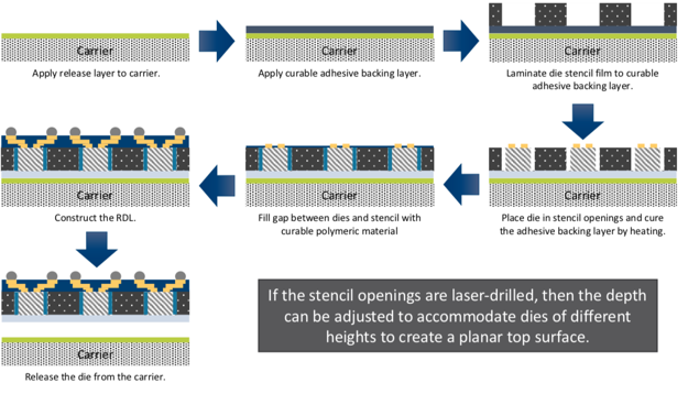
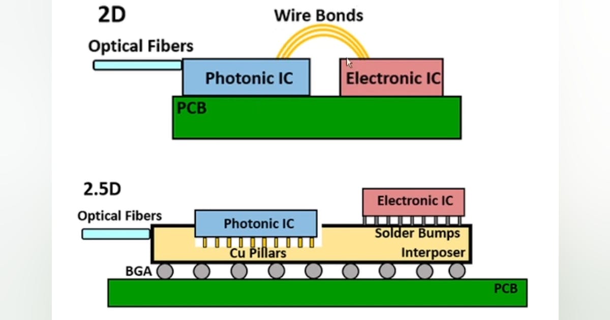
2 Example 25D Stacking Flow. Photonic Interconnects for Interposer-based 25D3D Integrated Systems on a Chip. Various Work Models P.
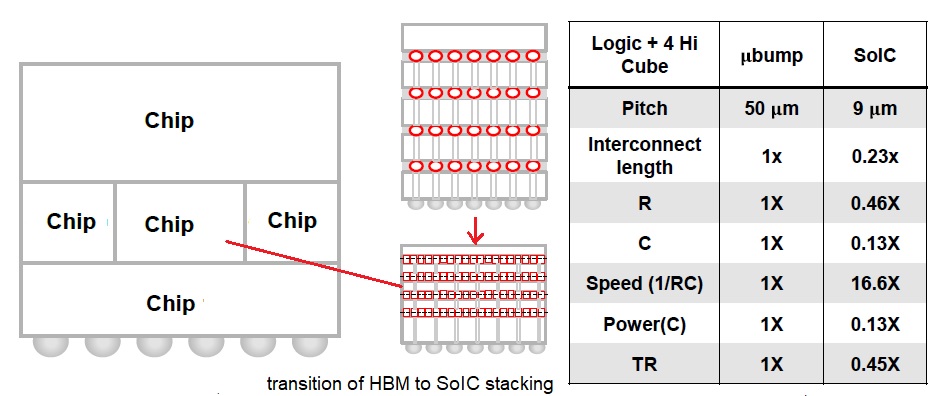
The following figure identifies the keywords Chiplet 25D 3D and SiP mentioned in this article for readers reference. Instead of a single die per chip package multiple dies stacked vertically 3D and placed on an interposer 25D is emerging as the building block for the future in both mobile and high-performance. The goal of our research in this thrust is to develop radical new 25D and 3D heterogeneous integration architectures for electronics photonics and mm-wave technologies.

Typical Structure Of 2 5d Ic Package Utilizing Interposer Not To Scale Download Scientific Diagram
Advanced 2 5d 3d Packaging Roadmap Semiwiki

Chip Packaging Part 4 2 5d And 3d Packaging Electronic Design

2 5d And 3d Ics New Paradigms In Asic Product Engineering Blog Einfochips

Financial Technology Isometric Flowchart Blockchain Crypto Money Flow Chart

A C 2 5d And 3d Mcm Integration Approaches Explored In Phase 1 D Download Scientific Diagram
2 5d Ic Integration Springerlink
Chip Packaging Part 4 2 5d And 3d Packaging Electronic Design

A C 2 5d And 3d Mcm Integration Approaches Explored In Phase 1 D Download Scientific Diagram

3018pro Power Milling Machine 3018pro In 2021 Cnc Engraving Machine Cnc Router Cnc Router Bits

Conquering 2 5d And 3d Chip Design Challenges With Monozukuri Semi

2 5d Chiplet Integration With An Interposer Download Scientific Diagram

Pin On Shop One B July 2019
More 2 5d 3d Fan Out Packages Ahead

2 5d 3d Chiplet Sip
2 5d Ic Integration Springerlink

2pack For Lg V20 Swezer Tempered Glass Screen Protector 9h Antichip Edge Antibubble An Tempered Glass Screen Protector Glass Screen Protector Screen Protector

2 5d Semiconductor Engineering

Samsung Announces Availability Of Its Next Generation 2 5d Integration Solution I Cube4 For High Performance Applications Techpowerup